During the course of the metallurgical analysis performed for our customers, we sometimes use the X-ray analysis capabilities of the EDS system, which works in conjunction with the Scanning Electron Microscope (SEM).
The Energy Dispersive X-Ray System makes use of the X-Ray spectrum emitted by a solid sample which has been bombarded with a focused beam of electrons. This electron beam is generated by the electron gun encased within the column of the Scanning Electron Microscope. When the electron beam interacts with the sample surface, secondary and backscattered electrons are emitted from the excited surface. 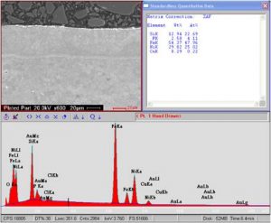 The topography revealed by the collected electrons is used to develop a CRT image of the sample surface. In addition, the wavelength and intensities of these collected electrons are analyzed and used to identify the element(s) contained within the near sample surface. The depth of the electron beam penetration is somewhat shallow, so surface preparation is important to a proper analysis. Most samples analyzed in this fashion are first subjected to metallographic mounting and polishing to insure a smooth, flat finish. These techniques are extremely useful in identifying and segregating plating and coating systems, as well as in identification of debris samples and general material and alloy identification.
The images above show the analysis of a hard nickel coating system on a steel part. Note how the scan and spectral map have properly identified the nickel-phosphorus precipitation hardening coating composition.
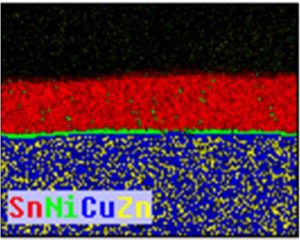 The following example is a prepared cross-section through a copper zinc alloy which has been tin coated. Note the well-defined nickel strike which is visible between the tin layer and Cu-Zn substrate. All of these layers can be accurately measured using the software of the SEM. In this case the nickel strike is approximately 0.25 microns thick (0.00001 inches). The flexibility of the system software allows us to combine individual elemental maps to obtain an image overlay as shown in the Sn-Ni-Cu-Zn photo at left.
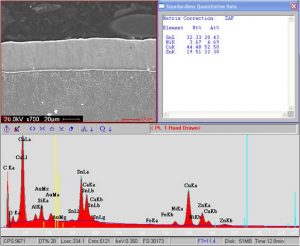 In this image, note the characteristic wavelength peaks displayed in the collected spectrum. These correspond to the atomic energy of the removed and collected electrons from the energized shell or subshell. The energies are measured in electron volts (eV) and for the purpose of these examinations we generally work in the range of 1 to 10 keV.
If you have questions about any of our metallurgical services or capabilities, please contact Walt Custer, Metallurgical Lab Manager at 937-298-9390 or via email.